CHN Awarded 2nd Patent
A 2nd Patent was awarded this month to CHN researchers Ahmed Busnaina, Siva Somu, & Cihan Yilmaz for “High rate electric field driven nanoelement assembly on an insulated surface”. Earlier this month, they were awarded a patent for "Nanoscale interconnects fabricated by electrical field directed assembly of nanoelements".
Abstract Source: USPTO
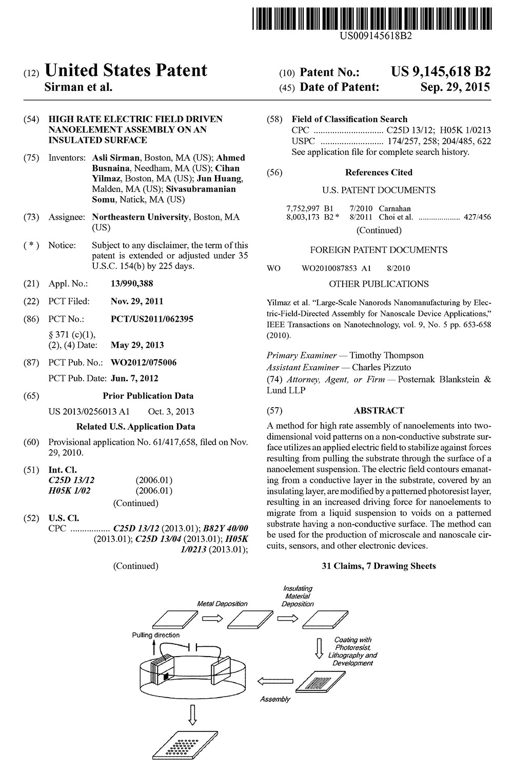
A method for high rate assembly of nanoelements into two-dimensional void patterns on a non-conductive substrate surface utilizes an applied electric field to stabilize against forces resulting from pulling the substrate through the surface of a nanoelement suspension. The electric field contours emanating from a conductive layer in the substrate, covered by an insulating layer, are modified by a patterned photoresist layer, resulting in an increased driving force for nanoelements to migrate from a liquid suspension to voids on a patterned substrate having a non-conductive surface. The method can be used for the production of microscale and nanoscale circuits, sensors, and other electronic devices.